Clarification regarding LED 4 on MitySOM-5CSX DevKit
Added by Judy Mastracco about 1 year ago
I am posting this on behalf of a customer.
I would like to verify that the schematic and pinout on MitySOM-5CSx_Pin-Out.xlsx, MitySOM-5CSx_Pin-Out.xlsx, MitySOM-5CSx_Pin-Out.xlsx documentation are up-to-date and specifically intended for the SoC model 5CSXFC6C6U23I7 used on the received MitySOM-5CSX evaluation board.
I’m asking because I created a small FPGA test project to deploy on the eval board, where the goal is simply to toggle a signal, but not the case ! I connected the main clock input to the output oscillator () 100MHZ HSMC2_CLK_P, which corresponds to pin T13 on the FPGA. However, when compiling with Quartus, I receive an error stating that this pin is not connected to a dedicated clock network (REFCLK/GCLK) accessible by the FPLL.
Thank you for your time and assistance.
Replies (11)
RE: Clarification regarding LED 4 on MitySOM-5CSX DevKit - Added by Michael Williamson about 1 year ago
I believe the spreadsheets are correct.
T13 is not connected to a dedicated clock input pin, needed to feed a REFCLK/CLK clock network. It is on pin 155 of the SOM connector.
HSMC2_CLK_P driving pin 155 of the Partial HSMC connector on the DevKit.
A coherent copy of this clock, GXB_REFCLK1_P, is fed to the SOM via pin 227 of the SOM interface, which is connected to pin P8 on the FPGA. You need to use that input if you are setting up a transceiver clocking interface to the Partial HSMC interface. We don't have a FPGA fabric general clock input pin connected to the partial HSMC connector. If you need to get a clock into the FPGA fabric, I would recommend you use the Full HSMC connector and drive HSMC1_CLKIN1_P or HSMC1_CLKIN2_P.
Please let me know if you still have questions.
-Mike
RE: Clarification regarding LED 4 on MitySOM-5CSX DevKit - Added by Anonymous fpga about 1 year ago
Thank you for your response. I’ve updated the clock pin configuration as suggested.
However, I’m currently facing an issue:
I have two MitySOM-5CSX evaluation boards. The binary I want to test is stored on the SD card. It works perfectly on the first MitySOM-5CSX board.
The second MitySOM-5CSX board has the same configuration (S100 switch settings), and I’m using the same SD card that works with the first one. But on the second board, the binary doesn’t run.
Any idea what could be causing this difference?
Thanks in advance for your help.
RE: Clarification regarding LED 4 on MitySOM-5CSX DevKit - Added by Daniel Vincelette about 1 year ago
Hello,
When you refer to the "binary," are you referring to the RBF file used to program the FPGA? If so, are you observing that the FPGA does not program correctly on the "bad" development kit—specifically, that the orange LED remains on (it should turn off once programming is successful)?
One possible cause for this issue is a mismatch in FPGA density between the two SOMs.
Could you please provide the full part number for both SOMs? You can find this on the white label on the back of each SOM. The part number format looks like this: 80-000642RC-3 (note that the number after the dash may vary depending on the revision).
Thank you,
Dan
JTAG programming issue on MitySOM-5CSX DevKit with Quartus (Windows 11) - Added by Anonymous fpga 8 months ago
Hello,
I’m trying to program a MitySOM-5CSX board via JTAG using Quartus on Windows 11, but I encounter an error immediately when starting the operation.
I'm using :
-Tool: Quartus [version], Windows 11
-Interface: USB-Blaster [I/II]
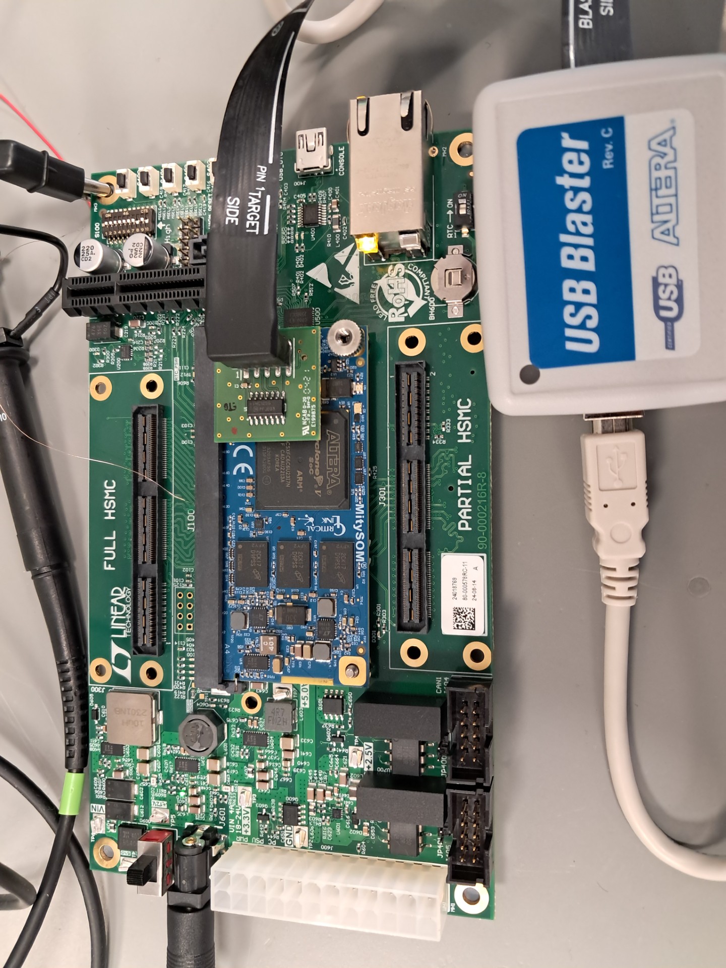
-Hardware: MitySOM-5CSX DevKit, connector J2
-Switch S100 configured as shown in the attached image (“S100_config.jpg”)
clipboard-202511121709-n8bnm.jpg
Steps Taken
- Connected the USB-Blaster to connector J2 on the DevKit.
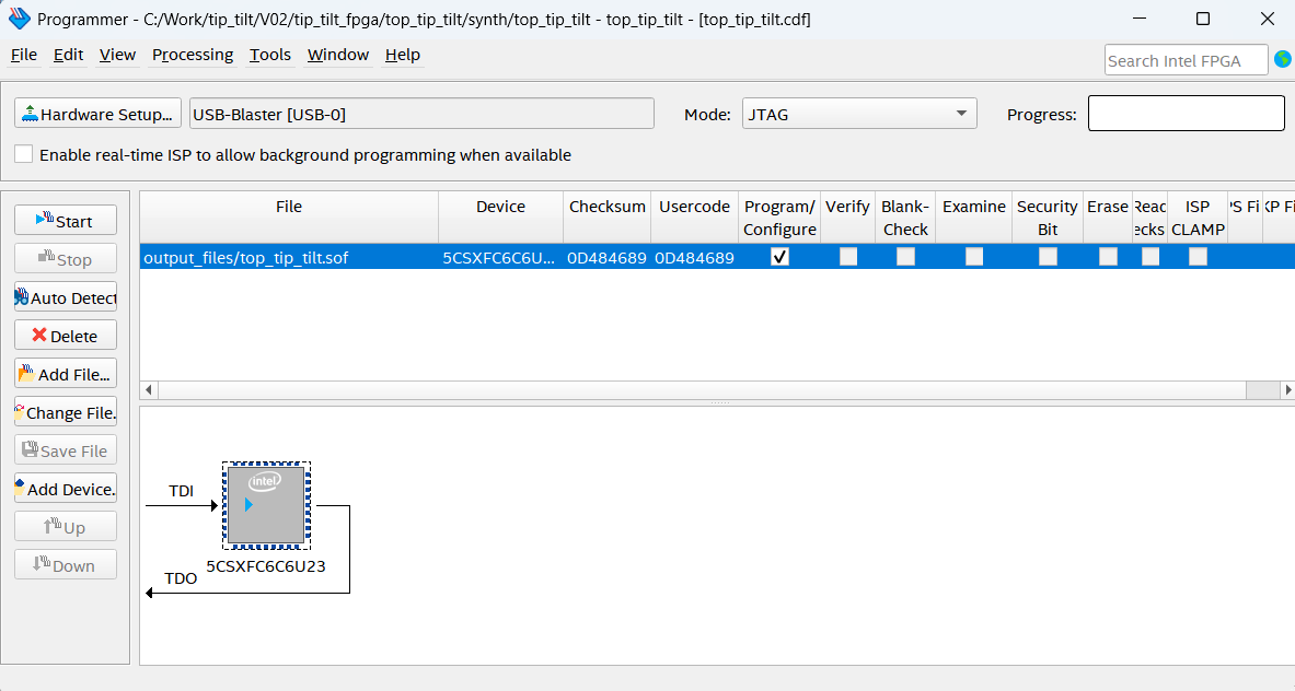
- Opened Quartus Programmer in JTAG mode as depicted in below picture.
clipboard-202511121710-lzxll.png
- Clicked Start to begin programming.
Result
Quartus displays the following error:
Info (209060): Started Programmer operation at Wed Nov 12 17:11:19 2025
Error (209040): Can't access JTAG chain
Error (209012): Operation failed
Info (209061): Ended Programmer operation at Wed Nov 12 17:11:21 2025
Could you please advise on possible causes and confirm whether the S100 switch settings and the J2 connection are correct for JTAG programming on this board?
Thank you in advance for your assistance.
Best regards
RE: Clarification regarding LED 4 on MitySOM-5CSX DevKit - Added by Mike Fiorenza 8 months ago
Atef,
From your picture, it looks like you have the JTAG pod plugged in backwards. Pin 1 on your ribbon cable does not align with Pin 1 on the JTAG adapter board.
Please try rotating your pod connection and report back.
- Mike
RE: Clarification regarding LED 4 on MitySOM-5CSX DevKit - Added by Anonymous fpga 8 months ago
Thank you Mike, the system works by reversing the USB Blaster connection. I have another question please: Do you have a tutorial that explains how to load the HPS portion using WSL on Windows? Thanks.
RE: Clarification regarding LED 4 on MitySOM-5CSX DevKit - Added by Mike Fiorenza 8 months ago
Atef,
Glad to hear you resolved your JTAG issue. Can you elaborate on how you are trying to load the HPS portion? Are you trying to load binaries directly to the HPS via JTAG? Unfortunately we do not have any tutorials at the moment that demonstrate that. Anything you do find online though for the Cyclone V should be applicable for that use case. Our tutorials load the HPS via the SD card.
RE: Clarification regarding LED 4 on MitySOM-5CSX DevKit - Added by Anonymous fpga 8 months ago
Mike, Thanks for your response. Yes, I was trying to load the compiled C code binary directly to the HPS via JTAG. Since there is no tutorial available for that method, could you please send me (or point me to) your tutorial explaining how to load the HPS via the SD card?
Thank you in advance for your help.
Best regards,
RE: Clarification regarding LED 4 on MitySOM-5CSX DevKit - Added by Mike Fiorenza 8 months ago
Atef,
If you see our Wiki page here: https://support.criticallink.com/redmine/projects/mityarm-5cs/wiki we post full SD card images for the development kits. These SD cards will use U-Boot as the bootloader which the HPS loads first then eventually loads into Linux. Within Linux, you could execute your C code binary on the HPS.
If you wanted to go the more bare metal approach, I would still start with our full SD card images which allow the HPS to load into the bootloader (U-Boot). Then within U-Boot, you can run the load mmc commands to load your bare metal .elf binary into memory from the SD card and then instruct the HPS to boot from it with the bootelf commands.
RE: Clarification regarding LED 4 on MitySOM-5CSX DevKit - Added by Anonymous fpga 8 months ago
Mike,
Thank you for your response, I’ll have a look at it.
I was focusing on using JTAG because I’m having an issue with SD-card boot on the carrier board I designed.
Thanks again for your help.
RE: Clarification regarding LED 4 on MitySOM-5CSX DevKit - Added by Mike Fiorenza 8 months ago
Atef,
Okay that makes sense! In that case, I would look into Arm Developer Studio then. You should be able to obtain an evaluation license and it should be able to accomplish what you are asking for. There are potential open-source solutions as well like OpenOCD, but may not be as full-featured.
https://developer.arm.com/Tools%20and%20Software/Arm%20Development%20Studio
https://openocd.org/

