EMIFA Interface
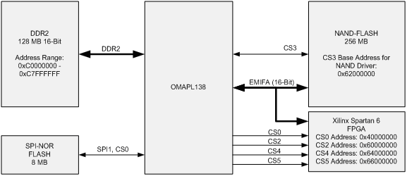
The memory interface for the MityDSP-L138F and MityARM-1808F SOMs is illustrated below. As shown in the figure, the SOM design uses chip select 3 (CS3) for interfacing to the on-board NAND devices. The remaining chip selects -- CS0, CS2, CS4, and CS5 -- are routed to the on-board Xilinx Spartan 6 FPGA. Critical Link provides a reference EMIFA framework that allows for installation of provided FPGA cores (e.g., UARTS, SPI busses, I2C, etc.) or user developed custom cores. This framework includes drivers for both the ARM (with linux OS) or the DSP (with BIOS OS) for the provided cores. This framework utilizes CS5 for all accesses, leaving the other chip selects available for customer use.
Users of the MityDSP-L138F family of SOMS are not required to use the Critical Link provided framework. It is provided for convenience only. If the architecture or wait states are not adequate for your design, you do not have to use it.

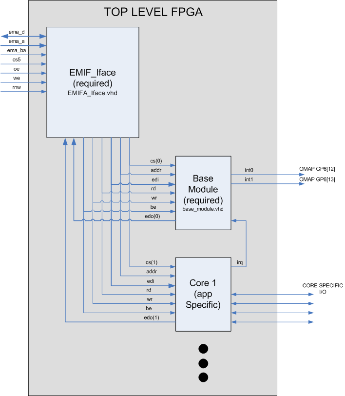
The figure below illustrates the FPGA top level block diagram of the EMIFA interface using the framework. From the diagram, there are two key modules used in the framework: the EMIFA_Iface module and the base_module module. Source code for both of these modules is included in the Board_Support_Package under the "fpga/vhdl" directory.

EMIFA_Iface
The EMIFA_Iface module provides the interface between the OMAP-L138 (or AM1808) EMIFA processor bus and the instantiated FPGA cores. It is responsible for decoding the chip select 5 address into a core-space chip select, providing a read and write strobe and multiplexing the core data bus outputs back to the OMAP-L138 processor bus. The EMIFA_Iface was designed to support a large number of cores bolted into the framework with a reasonably high (100 MHz) clock rate, and as such uses a fair number of pipelined registers during the decode/demuxing process.
EMIFA Interface Timing (Read Cycles)
The figure below illustrates the timing for an EMIFA read cycle as configured by the default u-Boot from Critical Link and through the CS5 framework (if used).
As shown in the figure, the EMIFA wait states for a read cycle for CS5 are:
- 1 Clock Setup
- 6 Clocks Read
- 1 Clock Hold
The signals, as illustrated in the figure correspond to the following FPGA fabric signals:
| Signal in Figure | Signal in FPGA | Signal at OMAP | Description |
| clk | Main ema_clk | clkout | This is the main EMIFA clockout signal from the OMAP |
| EMA_CS5_N | CS5 Input Pin | CS5 Output Pin | Chip select 5 active low |
| EMA_OE_N | OE Input Pin | OE Output Pin | Output enable active low |
| EMA_WE_N | WE Input Pin | WE Output Pin | Write Enable active low |
| cs5_n | clock CS5 input | N/A | this is a registered version of the CS5_N input |
| core_cs | Core Chip Select | N/A | this is the decoded chip select signal output by the EMIFA_Iface module to an FPGA core |
| EMA_D | EMIFA Data Output | EMIFA Data Input | The data driven on the EMIFA bus for a read |
Go to top

